Gain and offset problems of C&S ASIC
Facts:
The measures on the high gain channel showed quickly an important deviation
from design : a gain of approximately 60 instead of 96 and an offset around
-600 mV. These facts were reproduced entirely in the simulator by adding
parasitic resistors in several key connections (see figure below : parasitic
resistors on the high gain channel are drawn in dotted lines).
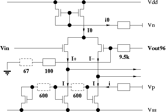
Explanation:
The parasitic resistor between the ASIC theoretical ground point and the
actual ground pad accounts for the decrease of gain, by modifying the bridge
resistor values. On the other hand, the first stage of the amplifier includes
two matched current sources that were supposed to subtract the same amount
of current I to the input transistor currents I+ and I-; the parasitic
resistors on their grid voltage inputs create an asymmetry, accounting
for the offset.
The origin of this problem lies in the design of the chip : the paths
to the ground pad and to the affected voltage supply are excessively convoluted,
to the point that the values of the parasitic resistors adopted for the
simulation are well in line with their actual geometries. This error could
not be detected by the design software, since the AMS 0.35 µm package
used for this chip does not take parasitic resistors into account, contrarily
to the previous one (a 0.6 µm package) used by our team.
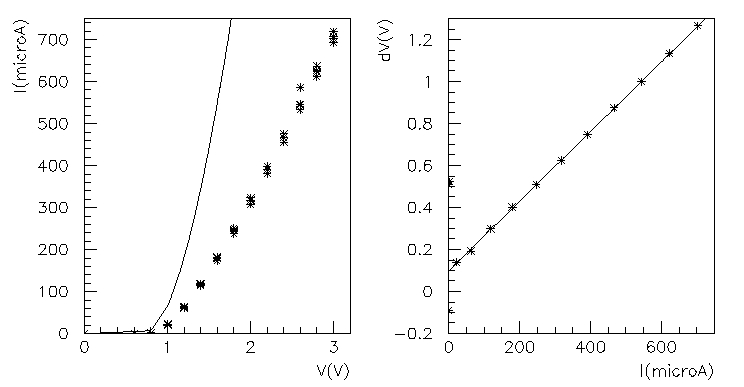
Verification:
On the experimental side, the existence of such resistors was proven with
by measuring the current-voltage curve on one transistor of the current
mirror. The plots below show the large difference between the simulated
and experimental current-voltage caracteristics, and the linearity of the
voltage difference as a function of the current. This matches what one
would expect with a large access resistor (around 1660 Ohm according to
this measure, comparable to the total of 1200 Ohm used in the simulation)
between the voltage measurement pad and the transistor.
Consequences:
Besides the change in gain and the important offset of the high gain channel,
this problem has other consequences affecting the noise analysis measurements
:
-
On both channels, there is a shift in pedestal between clamping and an
input of zero. The output during clamping is equivalent to an input of
-1 mV on both channel, and can be explained by a section of the grounding
parasitic resistor situated between the clamp 'grounding' point and the
actual ground pad (this resistor was actually measured during the linearity
studies).
-
The matched current sources problem increases strongly the sensitivity
of the offset to the power supply voltage : up to 0.2 mV offset variation
instead of a projected 5 µV for a 1 mV variation of the supply, on
the high gain channel. At its worst, power supply drift created a 5 µV
drift in pedestal level during a data acquisition run, exceeding the level
of noise we aimed at measuring.
Claire Juramy Last modified: September 9,
2004