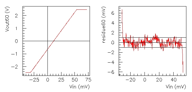
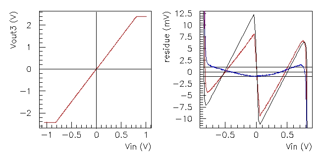
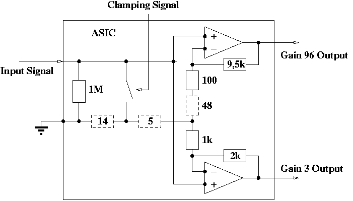
The plot of the residues from the linear fits is the key to judging the linearity of the amplifiers. In the case of the high gain amplifier, the residues show patterns generated by the ADC ; no deviation from linearity can be attributed to the amplifier. However, in the case of the low gain, the plot shows a clear pattern in the deviation from the linear fitting. A partial fit on each branch of that pattern shows a gain of 2.97 in the negative part, 2.98 in the positive part and only 2.75 in the central part of the +/-2.5 V interval. It should be noted that the different segments match exactly the different modes of the high gain channel, hence the idea to explain this apparent break in linearity by a coupling through the grounding parasitic resistor discussed in the previous section. If there is a resistance between the point where the resistor bridges of both gains are joined and the ground pad (see details on the schematic below), each output should create an additional voltage on the feedback input of the other amplifier.
The shape of the low gain residue graph was reproduced by simulating
such a configuration (black line in the residues graph). To eliminate this
coupling effect from our data and look at how the amplifier would work
without those parasitic resistors, we calculated a 'parasitic voltage',
created by the current coming from the high gain resistor bridge through
a part of the parasitic resistor. Then we calculated the effective input
and output voltages by subtracting this parasitic voltage to the measured
inputs and outputs. With a common resistor of 19 Ohm, out of a total 67
Ohm on the high gain channel, this operation effectively eliminated the
coupling pattern (blue line in the residues graph). This brought the residues
down to a reasonable level compared to the 12-bit ADC that will be used
for the integration into a readout chain. However, the remaining non-linearity
is not yet understood.